Using sound to test devices, control qubits

Acoustic resonators are everywhere. In fact, there is a good chance you’re holding one in your hand right now. Most smart phones today use bulk acoustic resonators as radio frequency filters to filter out noise that could degrade a signal. These filters are also used in most Wi-Fi and GPS systems.
Acoustic resonators are more stable than their electrical counterparts, but they can degrade over time. There is currently no easy way to actively monitor and analyze the degradation of the material quality of these widely used devices.
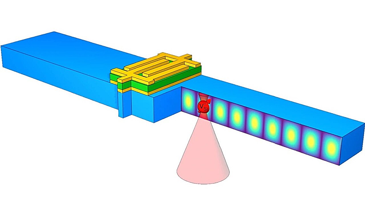
Now, researchers at the Harvard John A. Paulson School of Engineering and Applied Sciences (SEAS), in collaboration with researchers at the OxideMEMS Lab at Purdue University, have developed a system that uses atomic vacancies in silicon carbide to measure the stability and quality of acoustic resonators. What’s more, these vacancies could also be used for acoustically-controlled quantum information processing, providing a new way to manipulate quantum states embedded in this commonly-used material.
“Silicon carbide, which is the host for both the quantum reporters and the acoustic resonator probe, is a readily available commercial semiconductor that can be used at room temperature,” said Evelyn Hu, the Tarr-Coyne Professor of Applied Physics and of Electrical Engineering and the Robin Li and Melissa Ma Professor of Arts and Sciences, and senior author of the paper.
“As an acoustic resonator probe, this technique in silicon carbide could be used in monitoring the performance of accelerometers, gyroscopes and clocks over their lifetime and, in a quantum scheme, has potential for hybrid quantum memories and quantum networking.”
The research was published in Nature Electronics.
A look inside acoustic resonators
Silicon carbide is a common material for microelectromechanical systems (MEMS), which includes bulk acoustic resonators.
“Wafer-scale manufacturable silicon carbide resonators in particular are known to have the best-in-class performance for quality factor,” said Sunil Bhave, professor at the Elmore Family School of Electrical and Computer Engineering at Purdue and co-author of the paper. “But crystal growth defects such as dislocations and grain boundaries as well as resonator manufacturing defects such as roughness, tether stress, and micro-scale craters can cause stress-concentrations regions inside the MEMS resonator.”
Today, the only way to see what’s happening inside an acoustic resonator without destroying it is with super powerful and very expensive X-rays, such as the broad-spectral X-ray beam at the Argonne National Lab.
“These types of expensive and difficult-to-access machines are not deployable for doing measurements or characterization in a foundry or somewhere where you’d actually be making or deploying these devices,” said Jonathan Dietz, graduate student at SEAS and co-first author of the paper. “Our motivation was to try to develop an approach that would allow us to monitor the acoustic energy inside of a bulk acoustic resonator so you can then take those results and feed them back into the design and fabrication process.”
Silicon carbide commonly hosts naturally occurring defects in which an atom is removed from the crystal lattice, creating a spatially local electronic state whose spin can interact with sound waves through material strain, such as the strain generated by an acoustic resonator.
When acoustic waves move through the material, they put mechanical strain on the lattice, which can flip the spin of the defect. Changes in the spin state can be observed by shining a laser through the material to see how many defects are “on” or “off” after perturbing them.
“How dim or how bright the light indicates how strong the acoustic energy is in the local environment where the defect is,” said Aaron Day, a graduate student at SEAS and co-author of the paper. “Because these defects are the size of single atoms, the information they give you is very local and, as a result, you can actually map out the acoustic waves inside the device in this non-destructive way.”
That map can point to where and how the system may be degrading or not operating optimally.
Acoustic control
Those same defects in silicon carbide can also be qubits within a quantum system.
Today, many quantum technologies build on the coherence of spins: how long spins will remain in a particular state. That coherence is often controlled with a magnetic field.
But with their technique, Hu and her team demonstrated that they could control spin by mechanically deforming the material with acoustic waves, obtaining a quality of control similar to other approaches using alternating magnetic fields.
“To use the natural mechanical properties of a material—its strain—expands the range of material control that we have,” said Hu. “When we deform the material, we find that we can also control the coherence of spin and we can get that information just by launching an acoustic wave through the material. It provides an important new handle on an intrinsic property of a material that we can use to control the quantum state embedded within that material.”
More information:
Jonathan R. Dietz et al, Spin-acoustic control of silicon vacancies in 4H silicon carbide, Nature Electronics (2023). DOI: 10.1038/s41928-023-01029-4
Citation:
Using sound to test devices, control qubits (2023, October 25)
retrieved 26 October 2023
from https://techxplore.com/news/2023-10-devices-qubits.html
This document is subject to copyright. Apart from any fair dealing for the purpose of private study or research, no
part may be reproduced without the written permission. The content is provided for information purposes only.
For all the latest Technology News Click Here
For the latest news and updates, follow us on Google News.

