A transfer-printing technique to integrate metal electrodes and 2D materials on a wafer-scale

Metal-semiconductor junctions, electrical junctions in which a metal is linked to a semiconducting material, are crucial components for numerous electronic and optoelectronic devices. While they are now widely produced and used worldwide, creating good quality junctions that integrate conventional metals and 2D semiconductors can be difficult.
In fact, when applied to 2D materials, conventional metal deposition techniques, which entail a process known as ion bombardment, can cause a chemical disorder. In addition, existing transfer printing techniques, which involve the pre-deposition and transfer of metal electrodes on the surface of 2D materials, have been found to perform poorly due to the creation of chemical bonds on the substrate for the pre-deposition that hinder the electrodes’ transfer.
Researchers at the Chinese Academy of Sciences, Hunan University, City University of Hong Kong and Fudan University have recently developed a new technique that could be used to transfer metal electrodes on 2D materials more effectively, enabling the development of more reliable metal-semiconductor junctions. This technique, introduced in a paper published in Nature Electronics, entails the delamination of metal electrode arrays from a graphene wafer, and their subsequent transfer printing onto different 2D materials.
“For the first time, in 2013, we reported that continuous graphene monolayers can be grown via CVD directly on semiconducting Ge(001) surfaces, making a significant departure from conventional metallic systems,” Zengfeng Di, one of the researchers who carried out the study, told TechXplore. “Because of the insulating property of intrinsic Ge at the temperature below 10K, we carried out the research on graphene-mediated superconductivity in the metal nano-islands/graphene hybrid on Ge substrate, without the transfer of graphene from Ge substrate to SiO2 substrate.”
While conducting their previous research, Di and his colleagues realized that when deposited on graphene, metals can be peeled off very easily. This was also true for titanium or nickel, which are typically very difficult to exfoliate from conventional silica substrate.
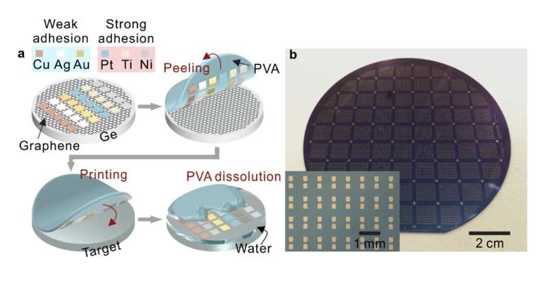
In their recent study, the team used their technique to deposit six different kinds of metals onto a wafer-scale graphene/Ge donor substrate. This included both weakly adhering metals, namely copper, silver and gold, and strongly adhering metals, namely platinum, titanium and nickel.

“Both weakly adhering metals and strongly adhering metals can be easily delaminated,” Di explained. “Our scalable, universal, and wafer-scale metal transfer technique can be utilized to create van der Waals contacts between two-dimensional semiconductors and three-dimensional metals, which are essential for developing 2D electronic and optoelectronic devices.”
The researchers’ approach for the integration of metal electrodes on 2D materials has several steps. First, it requires the deposition of a metal electrode array on a graphene/Ge substrate. As graphene is free from dangling bonds, the array can be easily peeled off from the substrate’s surface using a polymer film.
“After removing the polymer film by deionized water, wafer-scale 3D metal patterns can transfer onto an arbitrary target,” Di said. “Compared with the previous transfer printing methods using silica substrate, we can transfer arbitrary metal with 100% yield and scale up the transfer technology to wafer size.”
The approach developed by Di and his colleagues is universal and could be used to form van der Waals contacts between various 2D semiconductors and 3D metals. In the future, it could be used to realize new types of van der Waals integrated circuits.
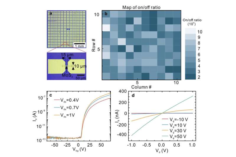
“A prerequisite for practical batch production of 2D devices is the ability of reliable mass production,” Di said. “With the graphene-assisted metal transfer-printing approach, we created MoS2 transistor arrays which show uniform electrical characteristics and good average values for the on/off current ratio, on-current, and subthreshold swing.”
Based on the initial tests they ran, Di and his colleagues think that their graphene-assisted metal transfer approach is a reliable solution for the large-scale manufacturing of integrated circuits based on 2D materials. In their next studies, they plan to start using their technique to develop specific components for electronic and optoelectronic devices, to evaluate its effectiveness further.
“Beyond a simple 2D transistor, we are using this technique to fabricate basic 2D logical units, including AND-OR, NOR, and AND gate,” Di added. “In addition, the cost of our approach should be further reduced by optimizing the process and increasing the reusability of graphene/Ge substrate.”
Guanyu Liu et al, Graphene-assisted metal transfer printing for wafer-scale integration of metal electrodes and two-dimensional materials, Nature Electronics (2022). DOI: 10.1038/s41928-022-00764-4
Gang Wang et al, Direct Growth of Graphene Film on Germanium Substrate, Scientific Reports (2013). DOI: 10.1038/srep02465
© 2022 Science X Network
Citation:
A transfer-printing technique to integrate metal electrodes and 2D materials on a wafer-scale (2022, June 20)
retrieved 20 June 2022
from https://techxplore.com/news/2022-06-transfer-printing-technique-metal-electrodes-2d.html
This document is subject to copyright. Apart from any fair dealing for the purpose of private study or research, no
part may be reproduced without the written permission. The content is provided for information purposes only.
For all the latest Technology News Click Here
For the latest news and updates, follow us on Google News.
