Breakthrough in enhancement of hole mobility in strained germanium leads to emergence of new class of quantum materials

Semiconductor materials are the foundation of modern electronic, photonic, photovoltaic, thermoelectric and many other semiconductor devices, which are integral for computers, mobile phones, gadgets, home appliances, cars and other equipment.
More than 99% of all semiconductor devices are made of or on silicon wafers. Novel group IV semiconductor epitaxial structures composed of silicon, germanium, carbon or tin on silicon or silicon-on-insulator wafers provide a natural route for continued improvement of properties of state-of-the-art silicon devices with enhanced or emerging unique properties.
Carriers’ mobility
Mobility of free carriers in conduction (electrons) or valance (holes) bands, along with a reasonably large energy bandgap, is one of the most important quality measures of any semiconductor material, determining its suitability for applications in a large variety of classical electronic, optoelectronic, and sensor devices, as well as for novel applications in emerging quantum devices.
Higher mobility enables faster operation of a device at lower power consumption and thus leads to reduced Joule heat dissipation, which is essential for scaling and increasing the speed of current electronic devices. It is even more important for those devices and electronics that work at cryogenic temperatures and are intended to control distributed registers of quantum processors. Also, carrier mobility is a critical quality for quantum devices, often playing a key role in new discoveries.
Strained germanium semiconductor
Germanium is a semiconductor material that has been used in the semiconductor industry since the invention of the first transistor. It has some advantages over other semiconductors such as silicon and various III-V compounds. In particular, if the mobility of the holes in germanium can be enhanced through strain engineering, this could lead to the development of new types of quantum materials with unique properties. Quantum materials are materials that exhibit unique electronic and magnetic properties due to their quantum nature, and they are being studied for a wide range of applications including quantum computing, sensing, and energy storage.
Semiconductor heterostructures on silicon have a built-in strain that is induced by the mismatch of the crystal lattices of the composed materials. It is an essential parameter used for energy band structure engineering of a material. But research and development of high mobility strained silicon, silicon-germanium and germanium heterostructures require special epitaxial growth techniques, like molecular beam epitaxy and chemical vapor deposition, combined with epitaxy knowledge and technologies in order to overcome various grand challenges in the heteroepitaxy of these materials.

Long-sought combination of parameters in one material system
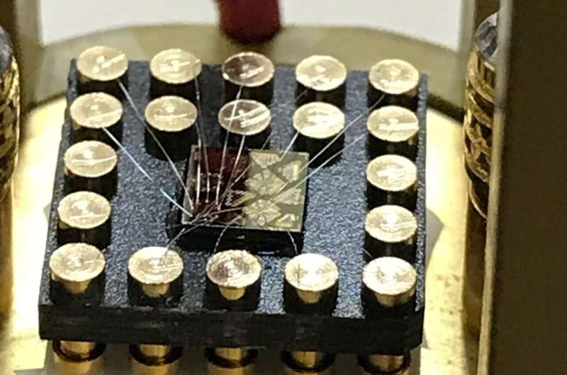
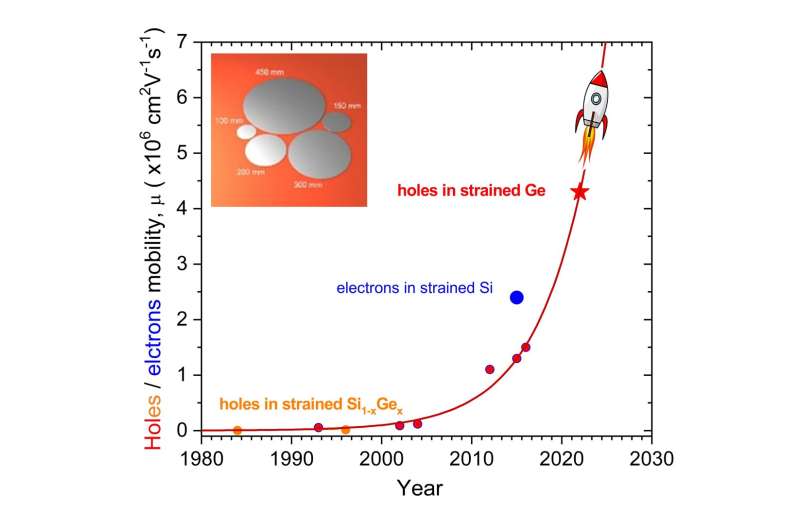
In our recent article, published in the journal Small Science, an international team of researchers from the U.K. and Canada reported on a record-high mobility of holes, reaching 4.3 million cm2V-1s-1 in an epitaxial strained germanium semiconductor, grown on a standard silicon wafer. This significant increase of the mobility by over four times, compared to the state of the art, allows holes to outperform electrons in the group-IV semiconductor materials. The demonstrated hole mobility in strained germanium is twice that of the best mobility of electrons reported in state-of the art strained silicon. A similar situation has not been observed for any other semiconductor material system.
In addition to the record mobility, this material platform reveals a unique combination of properties, which are a very large effective g*-factor, a low percolation density and a small effective mass. This long-sought combination of parameters in one material system is important for the research and development of low-temperature electronics with reduced Joule heating, and for quantum electronic circuits based on spin qubits, including devices for Majorana Fermions.
This major breakthrough was achieved due to the development of state-of-the-art epitaxial growth technology culminating in superior monocrystalline quality of the strained germanium material system with a very low density of background impurities and other imperfections. This superior material system with the combination of unique properties will lead to new opportunities for innovative quantum device technologies and applications in quantum as well as in classical electronics, optoelectronics, and sensors. In particular, the combination of obtained parameters will facilitate the realization of superior-quality laterally gated quantum devices. Moreover, these hole properties can be reliably simulated and predicted to reduce expensive and very time-consuming experimental trial-and-error attempts.
Comparison with other materials
This achievement reduces the gap between the best hole mobility in gallium arsenide heterostructures grown on the same material substrate, which was just recently increased from 2.3 million cm2V-1s-1 to 5.8 million cm2V-1s-1. Unfortunately, III-V materials are complicated to process, expensive, not widely abundant in the Earth’s crust compared to silicon and germanium, do not exist in isotopically pure forms, and are not compatible with the state-of-the-art silicon technologies for mass production. All other known semiconductors, including III-V, II-VI, perovskites, 2D materials, etc. show substantially lower hole mobility than in the strained germanium and gallium arsenide heterostructures.
We believe that the maximum mobility has still not been reached in the strained germanium heterostructures and there is room for further improvements. Clearly, more detailed experimental and theoretical studies are required to understand microscopic mechanisms that limit hole mobility.
Overall, this breakthrough in enhancing the mobility of holes in strained germanium could have significant implications for the development of new quantum materials and technologies. It will be exciting to see how this research progresses and what new applications emerge in the coming years.
This story is part of Science X Dialog, where researchers can report findings from their published research articles. Visit this page for information about ScienceX Dialog and how to participate.
More information:
Maksym Myronov et al, Holes Outperform Electrons in Group IV Semiconductor Materials, Small Science (2023). DOI: 10.1002/smsc.202200094
Maksym Myronov is a scientist, researcher and inventor. He is an Associate Professor and a group leader at The University of Warwick in the U.K. (warwick.ac.uk/MaksymMyronov). He is an expert in epitaxial growth, materials characterization and device technologies of group IV and III-V semiconductors. He has published more than 400 papers, including more than 150 articles in peer-reviewed international scientific journals, and four book chapters. He has given more than 150 talks at national and international conferences/workshops and has filed around 10 patents.
Citation:
Breakthrough in enhancement of hole mobility in strained germanium leads to emergence of new class of quantum materials (2023, May 4)
retrieved 4 May 2023
from https://techxplore.com/news/2023-05-breakthrough-hole-mobility-strained-germanium.html
This document is subject to copyright. Apart from any fair dealing for the purpose of private study or research, no
part may be reproduced without the written permission. The content is provided for information purposes only.
For all the latest Technology News Click Here
For the latest news and updates, follow us on Google News.

