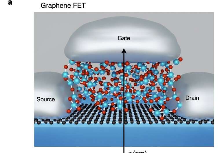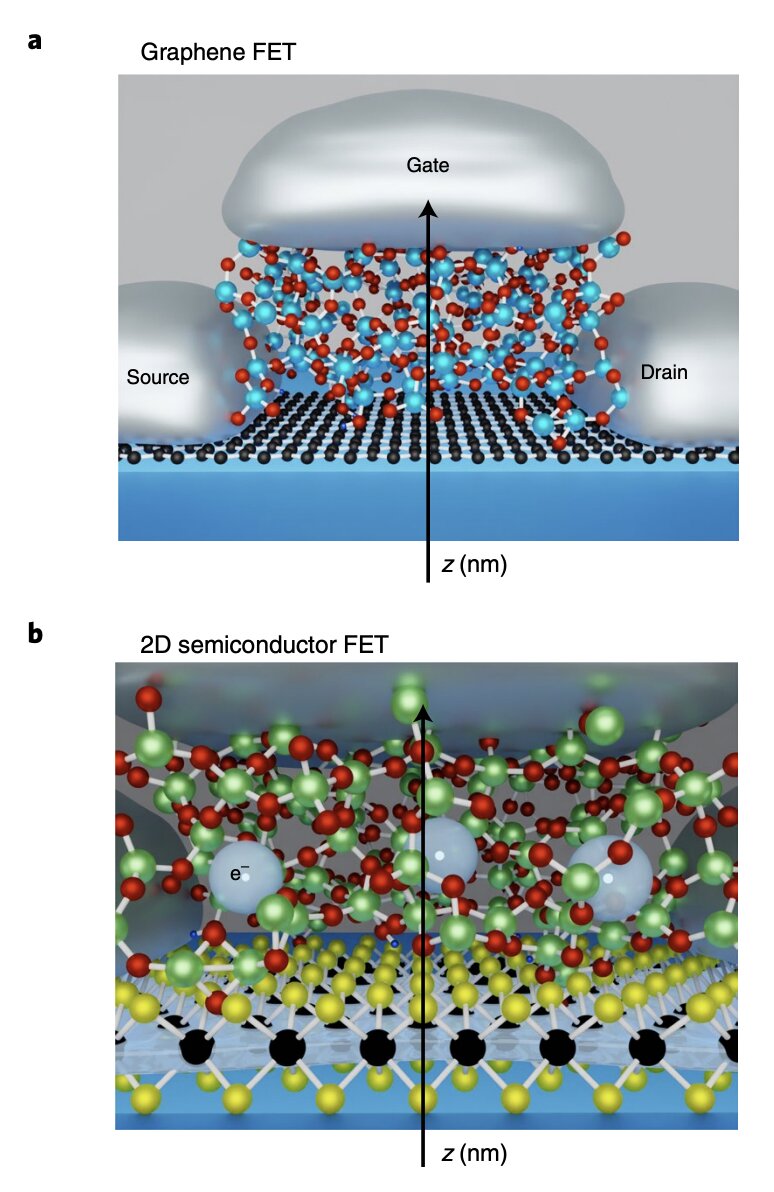
Two-dimensional (2D) semiconductors are a class of semiconducting materials with thicknesses on the atomic scale. These materials have numerous advantageous properties, including good mobilities at thicknesses below 1 nm, which make them particularly promising for the development of field effect transistors (FETs) and other electronic, photonic and optoelectronic components.
Despite their advantages, when they are used to build electronic components, these materials often exhibit a limited electrical stability. The main reason for this is that the charge carriers originating from the semiconductors can interact with defects in the insulators that surround the materials inside devices, hindering the devices’ stability.
Researchers at TU Wien and AMO GmbH have recently demonstrated a strategy that could be used to improve the stability of FETs based on 2D materials. This strategy, introduced in a paper published in Nature Electronics, entails tuning the Fermi Level of the 2D materials, ensuring that it maximizes the energy distance between the charge carriers and defects in the gate insulator while the device is operating.
“In FETs, the resulting trapped charges can lead to large hysteresis and device drifts, particularly when common amorphous gate oxides (such as silicon or hafnium dioxide) are used, hindering stable circuit operation,” the researchers wrote in their paper. “We show that device stability in graphene-based field-effect transistors with amorphous gate oxides can be improved by Fermi-level tuning.”
In their experiments, the researchers tested different graphene FETs with aluminum oxide (Al2O3) as the top-gate oxide and compared their performances. One of the device batches they tested also utilized a p-doped graphene layer.
“We deliberately tuned the Fermi level of the channel to maximize the energy distance between the charge carriers in the channel and the defect bands in the amorphous aluminum gate oxide,” the researchers explained in their paper.
Interestingly, the researchers found that their approach improved the stability of the transistors. In fact, the batch of FETs that was Fermi tuned away from the aluminum oxide’s defects (i.e., the one that was most p-doped) resulted in lower hysteresis and bias temperature instability, two characteristics typically associated with operational instability.
The team verified the effectiveness of their approach further by running a series of technology computer-aided design (TCAD) simulations. These are computer simulations often used to model semiconductor devices and processes.
“Charge trapping is highly sensitive to the energetic alignment of the Fermi level of the channel with the defect band in the insulator, and thus, our approach maximizes the amount of electrically active border traps without the need to reduce the total number of traps in the insulator,” the researchers added in their paper.
The recent work by this team of researchers highlights the need to choose suitable designs for devices based on 2D semiconductors to ensure reliable and stable operation. In the future, the approach introduced in their paper could be used to improve the stability of FETs based on 2D graphene.
Moreover, the same strategy could potentially be applicable to a wide range of insulators, including crystalline insulators. In their next studies, the researchers plan to test their proposed strategy further, to determine the levels of stability that it could enable with different material combinations.
Building up new data-storage memory
Theresia Knobloch et al, Improving stability in two-dimensional transistors with amorphous gate oxides by Fermi-level tuning, Nature Electronics (2022). DOI: 10.1038/s41928-022-00768-0
© 2022 Science X Network
Citation:
Fermi-level tuning to improve the stability of 2D graphene-based FETs (2022, June 28)
retrieved 28 June 2022
from https://techxplore.com/news/2022-06-fermi-level-tuning-stability-2d-graphene-based.html
This document is subject to copyright. Apart from any fair dealing for the purpose of private study or research, no
part may be reproduced without the written permission. The content is provided for information purposes only.
For all the latest Technology News Click Here
For the latest news and updates, follow us on Google News.

