


Photodetectors, sensors that can detect light or other forms of electromagnetic radiation, are essential components of imaging tools, communication systems, and various other technologies on the market. These sensors work by converting photons (i.e., light particles) into electrical current.
Researchers at Zhejiang University have recently developed a new photodetector that could detect light within a broader bandwidth. Their device, presented in a paper published in Nature Electronics, could be used to develop new and more advanced imaging technologies.
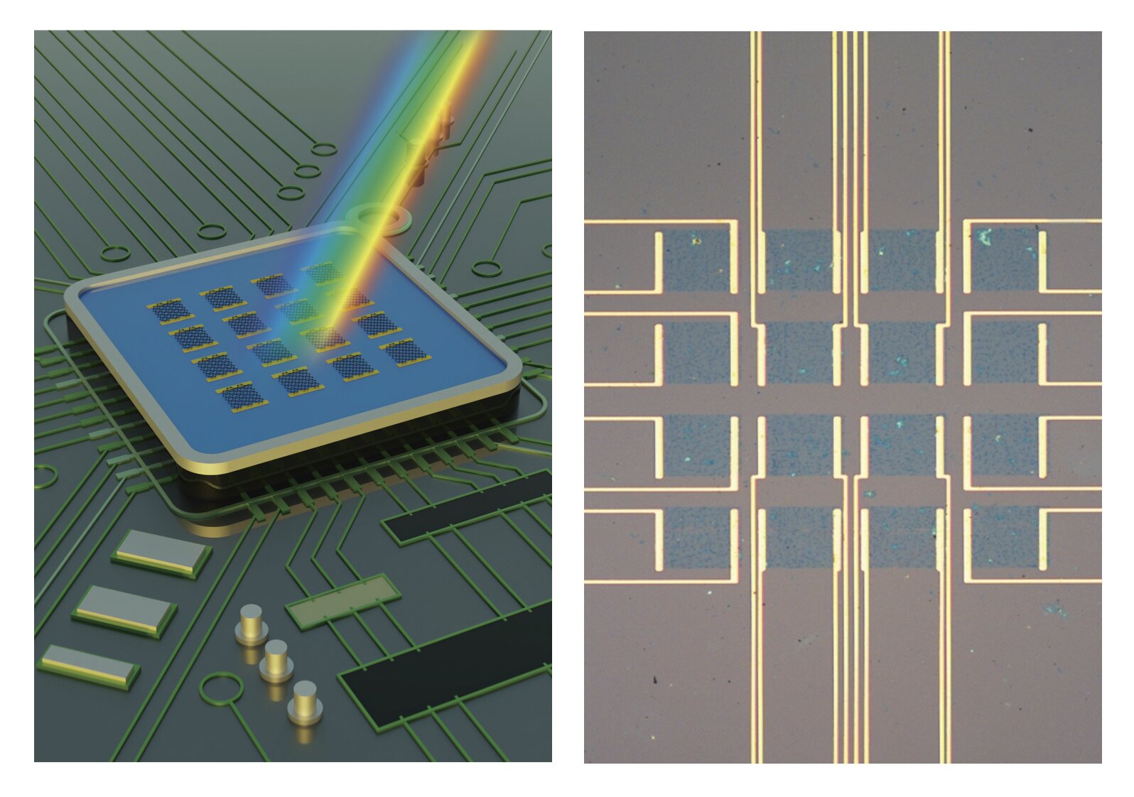
“Our recent project is based on traditional charge-coupled device (CCD) and complementary metal-oxide-semiconductor (CMOS) imaging technologies,” Prof. Yang Xu, one of the researchers who carried out the study, told TechXplore. “Our novel imaging devices combining CCD’s MOS photogate for high sensitivity and CMOS’s independent pixel structure can significantly benefit monolithic integration, performance, and readout.”
Typically, CCD and CMOS imagers based on silicon (Si) can only detect light in the visible range, due to their intrinsic bandgap absorption limit. Xu and his colleagues were able to broaden the bandwidth of the light that can be picked up by their photodetector by incorporating graphene into it.
“Our goal was to improve the responsivity and spectral performance of Si-based image sensors,” Xu explained. “First, we formed a Schottky junction between the Si and the multilayer graphene (MLG), where the IR-light induced hot holes in MLG are injected into Si (n-type) under the electrical field of Vg via photo-thermionic (PTI) emission. Second, we formed a deep-depletion well in the SiO2/Si interface under the voltage pulse, storing and integrating photo-charges.”
Ultimately, the researchers placed single-layer graphene (SLG) on top of the oxide in their device. This layer ultimately allows the photodetector to directly and non-destructively read out the carriers stored in the deep depletion well through the photogate effect, which is caused by the graphene’s strong field.
“The design of our proposed device realizes in-situ pixel-level readout of the charges in the profound depletion potential well, avoiding the sequential charge transfer in traditional CCD devices,” Xu said. “In addition, we broadened the detection bandwidth to IR by integrating a MLG charge injection path at the bottom of the device.”
In initial tests, Xu and his colleagues found that their photodetector’s detection bandwidth is significantly broader than that of traditional Si-based devices, which typically only detect light in the visible wavelength. As it integrates a readout channel SLG, a Si-based deep depletion well and a charge injection layer (MLG), the device could be particularly valuable for imaging applications with high-density integration.
“Our paper solves two crucial problems, by replacing sequential charge transfer with direct readout, which simplifies the architecture and data processing, while also broadening the response range to IR by infrared charge injection,” Xu said. “I also would like to thank our collaborators, Prof. Chao Gao, Prof. Xiangfeng Duan, Prof. Xiaomu Wang, Prof. Tawfique Hasan, Prof. Zhipei Sun and Prof. Bin Yu for their significant contribution.”
In the future, the photodetector developed by this team of researchers could be used to develop imaging devices for broadband image fusion, computer vision, robots, and various other applications. In their paper, Xu and his colleagues also briefly outline a series of suggestions for designing circuits that could enable the integration of their devices with new or existing technology.
“In our next studies, we will focus more in depth on the integration of our devices,” Xu added. “Our devices can perform the pixel information storage function via the storage of light-induced carriers in the potential well. This, combined with the tunable responsivity, could potentially prove valuable for building neuromorphic devices.”
Wei Liu et al, Graphene charge-injection photodetectors, Nature Electronics (2022). DOI: 10.1038/s41928-022-00755-5
© 2022 Science X Network
Citation:
Graphene charge-injection photodetectors with a broader detection bandwidth (2022, June 10)
retrieved 10 June 2022
from https://techxplore.com/news/2022-06-graphene-charge-injection-photodetectors-broader-bandwidth.html
This document is subject to copyright. Apart from any fair dealing for the purpose of private study or research, no
part may be reproduced without the written permission. The content is provided for information purposes only.
For all the latest Technology News Click Here
For the latest news and updates, follow us on Google News.