India’s Techade: AMD opens its largest global design centre in Bengaluru in a major boost for India Semicon
![]()
As part of its plan to invest $400 million over the next five years in India, AMD has built its largest R&D centre in Bengaluru, called Technostar research and development campus
AMD has officially inaugurated its largest global design centre, the Technostar research and development campus, in Bengaluru, India.
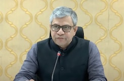
The inauguration ceremony was attended by Ashwini Vaishnaw, the Union Cabinet Minister for Railways, Telecommunications, Electronics, and Information Technology, along with Mark Papermaster, CTO of AMD, and other top AMD executives.
Related Articles

Fighting Deepfakes: MeitY, social media reps formulate plan to take on AI-gen fake videos

India’s mobile phone manufacturing at $44 billion, exports at $11 billion, says IT Minister Vaishnaw
The Technostar campus is part of AMD’s $400 million investment over the next five years in India, as announced at Semicon 2023.
Covering 500,000 square feet, the campus is expected to accommodate around 3,000 engineers and will focus on the development of CPUs, GPUs, adaptive SoCs, and FPGAs for personal computers and data centres.
The inauguration aligns with India’s semiconductor program, emphasizing support for the semiconductor design and talent ecosystem.
The facility includes a modern research and development lab, a demo centre for visitors, and collaborative huddle spaces. With 25 per cent of AMD’s global workforce based in India, the new design centre is anticipated to play a significant role in advancing semiconductor technologies.
Mark Papermaster, the EVP and CTO of AMD, highlighted the company’s commitment to engineering excellence and innovation, stating that the new design centre will contribute to technology and product development across AMD’s portfolio, supporting the next generation of high-performance, adaptive, and AI computing solutions globally.
(With input from agencies)
For all the latest Technology News Click Here
For the latest news and updates, follow us on Google News.
