Irregular or unexpected behavior in new thin-film transistors shouldn’t negate that research direction
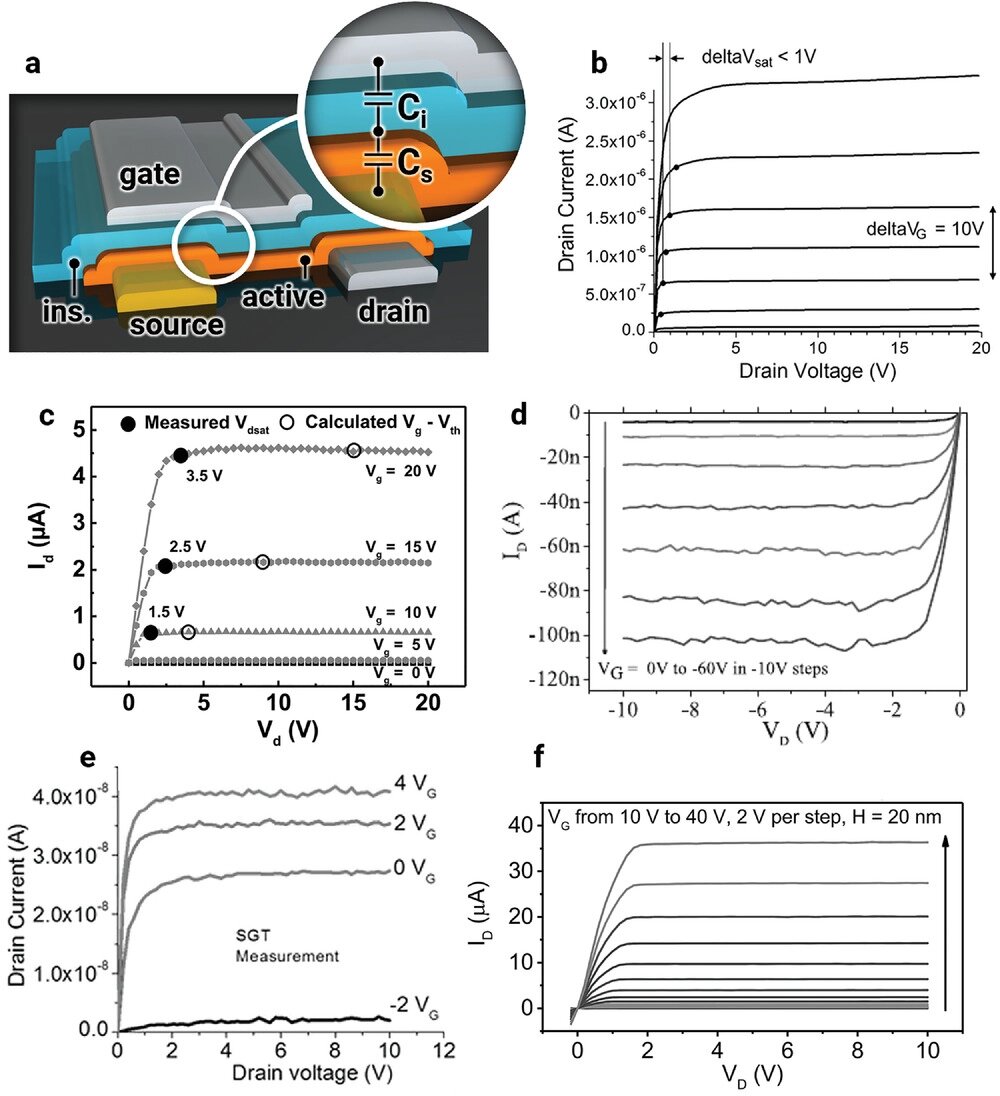
![Figure 1. Source-gated transistor (SGT) structure and output characteristics. a) Schematic cross-section of a staggered top-gate SGT, emphasizing the capacitive divider at the edge of the source in the inset. Output characteristics from published literature, in various material systems, reproduced with permission: b) low temperature polysilicon (LTPS) SGT (reprinted from Ref. [9] under the Creative Commons CC-BY-NC-SA license); c) InGaZno (IGZO) with graphene contact SGT (reprinted from Ref. [28] with the permission of AIP publishing); d) silicon nanowire (Si NW) SGT (reprinted from Ref. [29] under the Creative Commons CC BY license); e) ZnO nanosheet (NS) SGT (reprinted from Ref. [30] under the Creative Commons CC BY license); f) IGZO SGT with Schottky contact (reprinted from Ref. [16] under the Creative Commons CC BY license). Credit: DOI: 10.1002/aelm.202101101 Irregular or unexpected behavior in new thin-film transistors shouldn't negate that research direction](https://scx1.b-cdn.net/csz/news/800a/2021/irregular-or-unexpecte.jpg)
Researchers from the University of Surrey and the Max Planck Institute in Stuttgart, Germany, have arrived at a set of recommendations that may see an explosion in the research effort into unconventional electronic devices.
Transistors are the small electronic switches and amplifiers that make up the electronic circuits that underpin all modern technologies. Thin-film transistors (TFTs) are made with low-cost materials and techniques, which means large-area circuits can be made economically. Typical uses are in display screens and imaging arrays and a multitude of emerging sensors and wearable applications.
Often, when scientists exploring new material combinations for creating TFTs encounter irregular or unexpected behavior, they abandon that research direction and look at different materials. However, the findings by the Surrey-led team suggest their change in tack could be premature, and they might be missing an important line of investigation. Some characteristics of inefficient TFTs could be hallmarks of unoptimised source-gated transistor (SGT) behavior. SGTs, a class of TFTs invented and perfected at the University of Surrey, score poorly in the usual metrics of TFT performance but have significant amplification and uniformity advantages, making them useful in an increasing number of emerging applications, for example imperceptible technologies and environmental sensors.
In their recent publication in the Advanced Electronic Materials journal, the research team give numerous examples that demonstrate cases in which underwhelming TFT behavior may be turned into high-performance SGT operation. They share the secret ingredient which is often overlooked but is crucial to ensuring successful transistor realization, specifically the relative electrostatic properties of the semiconductor and insulator layers in the critical region of the transistor. They recommend doing the following:
- First, researchers need to create a high enough source barrier to ensure that the source region is significantly more resistive than the channel in all biasing conditions. This is a requirement for SGT functionality.
- Critically, choose the material and thickness of the active and insulator layers so that the saturation coefficient is kept well below 0.3, ideally close to 0.1, to allow amplification to occur from low voltages.
- Maintain source-gate overlap to at least 100x semiconductor thickness to ensure that drain current is dominated by charge injection from the bulk of the source, reducing the transistor’s susceptibility to temperature and to variations during manufacturing.
- Build a lateral field relief structure into the source electrode to improve saturation, further increasing the amplification performance.
Dr. Hagen Klauk at the Max Planck Institute said:
“While it is almost always preferable to attempt to obtain ideal contact properties, it is not always possible. Even then, useful functionality can be derived by thoughtful matching of materials and processes to the desired application requirements. Engineers now have the option to optimize for switching performance or for some other desirable property. It has taken many years and numerous researchers’ efforts to bring thin-film transistor technology to its current state. There may be a long but interesting road ahead for the development of non-standard devices.”
Dr. Radu Sporea, senior lecturer at Surrey’s Advanced Technology Institute, said:
“The recent surge in publications that report source-gate transistors in varied material systems hints at how popular this type of transistor can become. It is very likely that many other experiments have been cut short when the expected thin-film transistor operation was not achieved, overlooking the opportunity for creating excellent SGTs in the process. We believe that many research groups will find our recommendations a useful reference for designing high-performance electronic systems, well beyond the current vision for the Internet of Things.”
Simplified circuit design could revolutionize how wearables are manufactured
Eva Bestelink et al, The Secret Ingredient for Exceptional Contact‐Controlled Transistors, Advanced Electronic Materials (2021). DOI: 10.1002/aelm.202101101
Citation:
Irregular or unexpected behavior in new thin-film transistors shouldn’t negate that research direction (2021, December 16)
retrieved 16 December 2021
from https://techxplore.com/news/2021-12-irregular-unexpected-behavior-thin-film-transistors.html
This document is subject to copyright. Apart from any fair dealing for the purpose of private study or research, no
part may be reproduced without the written permission. The content is provided for information purposes only.
For all the latest Technology News Click Here
For the latest news and updates, follow us on Google News.

