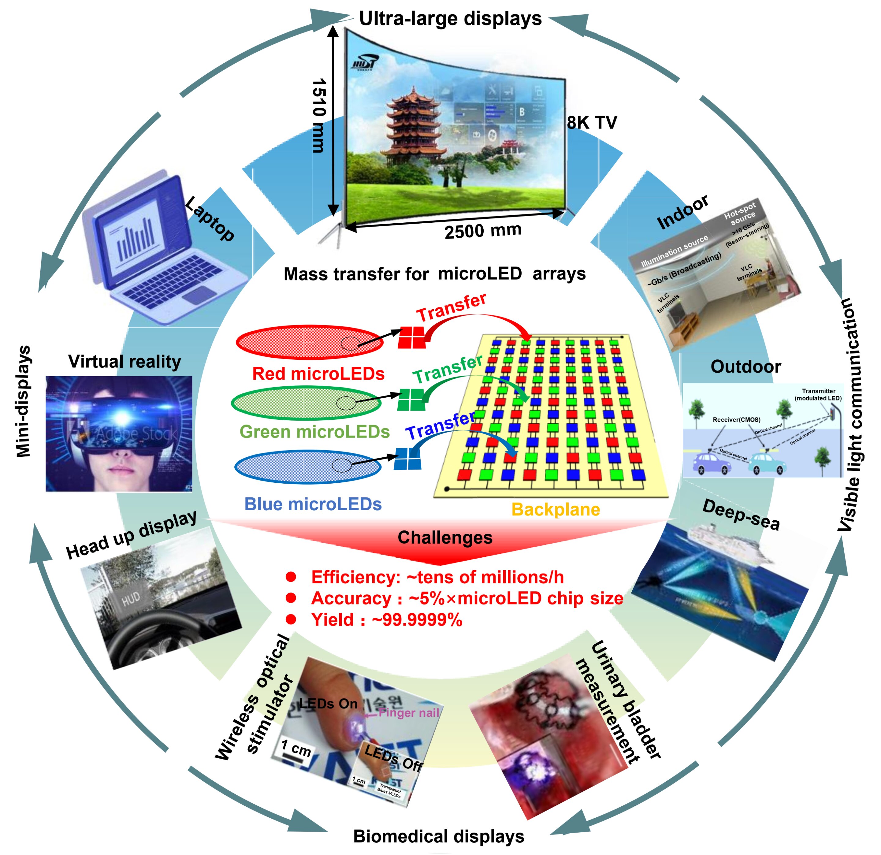
 and representative applications that have been described above. Deterministic assembly of microLED chips from different growth/donor substrates is required. However, since the feature size of microLED chips is <100 µm, there is a trade-off between tiny feature size and fabrication feasibility. There are three enormous challenges. 1) The extreme transfer efficiency (~tens of millions/h) is vital because of their vast numbers. 2) The extreme placement accuracy (~ 5% of the microLED chip size) is critical for microscale chips. 3) The extreme reliability (~99.9999% ) is also essential. In short, traditional assembly methods are not practical for MicroLEDs, and new integration technologies need to be developed. Credit: By Furong Chen, Jing Bian, Jinlong Hu, Ningning Sun, Biao Yang, Hong Ling, Haiyang Yu, Kaixin Wang, Mengxin Gai, Yuhang Ma and YongAn Huang")
Recent impressive advances in mass transfer techniques have proven to be a promising solution to overcome the extreme requirements of assembling microLED chips, including the laser lift-off technique, contact µTP technique, laser non-contact µTP technique and self-assembly technique.
The development of these advanced mass transfer techniques also provides an evaluation of microLED display techniques for applications in ultra-large displays, flexible electronics and visible light communications.
In a new paper published in the International Journal of Extreme Manufacturing, a team of researchers, led by Dr. YongAn Huang from State Key Laboratory of Digital Manufacturing Equipment and Technology, Flexible Electronics Research Center, Huazhong University of Science and Technology, PR China, have summarized comprehensively the extreme processes and applications of mass transfer techniques.
The main aim of this review is to address the latest developments in mass transfer techniques and widespread applications in microLED displays. The general assembly process of microLED displays and the highlight of key challenges of mass transfer techniques have been discussed first. Thereafter, various state-of-the-art mass transfer strategies and principles adopted in different production steps (i.e., epitaxial Lift-off technique and pick-and-place technique) of microLED displays are described. Finally, future research directions and opportunities are discussed in terms of transfer mechanisms, reliability, and cost effects.
Professor YongAn Huang (Huazhong University of Science and Technology) provides an outlook on the future research and applications needed for mass transfer:
“A further in-depth study of interfacial adhesion mechanisms is necessary. The essential relationship between the process parameters and interface reaction (e.g., adhesion strength, fracture mechanics, and chip peeling/flighting state) can undoubtedly provide quantitative guidance for the high reliability of mass transfer.”
“Although lots of small-area transfer schemes have been extensively verified, a further improvement in the reliability, accuracy, and efficiency of large-area transfer techniques is still an area of tremendous opportunities.”
“For achieving high reliability, the development of high precision micro-fabrication/position technologies and material preparations for chips, transfer stamps, and receiver substrates/solders are hotspots. Since lots of mass transfer techniques rely on some specific properties/shapes at specified positions. For example, the fluid self-assembly technique has special requirements for adhesives, which ask for better fluidity, high bonding selectivity between assembled and unassembled surfaces, and acid/high-temperature resistance considering subsequent processes.”
“Further exploration of cost-efficient mass transfer techniques is full of challenges as well as opportunities. The development of reversible laser-assisted μTP has important practical significance, which can easily achieve high throughput for large-scale and high-output manufacturing with the help of parallel laser systems and automated platforms.”
Furong Chen et al, Mass transfer techniques for large-scale and high-density microLED arrays, International Journal of Extreme Manufacturing (2022). DOI: 10.1088/2631-7990/ac92ee
Provided by
International Journal of Extreme Manufacturing
Citation:
Mass transfer techniques for large-scale and high-density microLED arrays (2022, November 15)
retrieved 15 November 2022
from https://techxplore.com/news/2022-11-mass-techniques-large-scale-high-density-microled.html
This document is subject to copyright. Apart from any fair dealing for the purpose of private study or research, no
part may be reproduced without the written permission. The content is provided for information purposes only.
For all the latest Technology News Click Here
For the latest news and updates, follow us on Google News.