Neuromorphic semiconductor device achieves world’s highest handwriting pattern recognition rate

A research team led by Dr. Yong-hun Kim and Dr. Jeong-Dae Kwon has successfully developed the world’s first neuromorphic semiconductor device with high-density and high-reliability by developing a thin film of lithium-ion battery materials. They achieved this by producing ultra-thin lithium ions, a key material of lithium-ion batteries that have been in the spotlight recently, and combining it with two-dimensional nano-materials. The research team is from the Surface & Nano Materials Division at the Korea Institute of Materials Science (KIMS).
A neuromorphic semiconductor device has synapses and neurons similar to the human brain, which processes and memorizes information. The synaptic device receives signals from neurons and modulates the synaptic weight (connection strength) in various ways to simultaneously process and store information. In particular, the linearity and symmetry of synaptic weights enables various pattern recognition with low power.
Traditional methods for controlling synaptic weights use charge traps between interfaces of heterogeneous materials or oxygen ions. In this case, however, it is difficult to control the movement of ions in the desired direction according to the external electric field. The researchers solved this problem with an artificial intelligence semiconductor device with high density by developing a thin film process while maintaining the mobility of lithium ions according to the external electric field. The thin film—with a thickness of several tens of nanometers—enables fine pattern processing while controlling the thickness of the wafer scale.
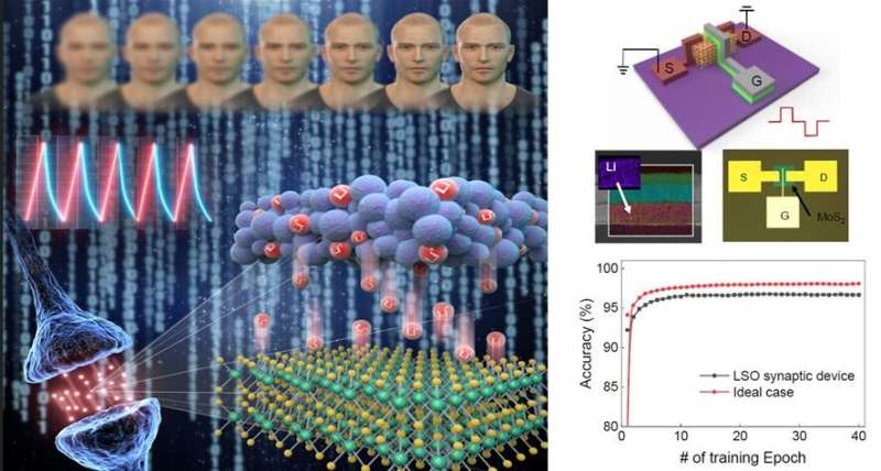
The research team developed the film using a vacuum sputtering deposition method that is used in general semiconductor processing. The thickness of the deposited film is less than 100 nanometers. After a transistor-type device on a silicon wafer substrate is manufactured and when an electric field is applied from the outside, the lithium ions in the charged lithium thin film move so that the conductivity of the channel can be precisely controlled.
The research team implemented an artificial neural network learning pattern using this synapse device and developed handwriting image pattern recognition. The artificial intelligence semiconductor device shows a handwriting pattern recognition rate of about 96.77% by maintaining the characteristics of finely adjusted synaptic weight even in an electric field repeated more than 500 times.
The research team stated, “Our next-generation neuromorphic semiconductor device does not require CPU and memory, the traditional Von Neumann-type information processing device and information storage device. It can simultaneously process and store information and learns and recognizes images such as handwriting patterns. It is expected to be applied to various low-power artificial intelligence devices such as world-class neuromorphic hardware systems, haptic devices, and vision sensors.”
The results of the research were published in ACS Applied Materials & Interfaces on November 17, 2022. The research team is conducting follow-up research on low-power artificial intelligence devices and wearable edging devices.
More information:
Byeongjin Park et al, Robust 2D MoS2 Artificial Synapse Device Based on a Lithium Silicate Solid Electrolyte for High-Precision Analogue Neuromorphic Computing, ACS Applied Materials & Interfaces (2022). DOI: 10.1021/acsami.2c14080
Provided by
National Research Council of Science & Technology
Citation:
Neuromorphic semiconductor device achieves world’s highest handwriting pattern recognition rate (2023, February 20)
retrieved 20 February 2023
from https://techxplore.com/news/2023-02-neuromorphic-semiconductor-device-world-highest.html
This document is subject to copyright. Apart from any fair dealing for the purpose of private study or research, no
part may be reproduced without the written permission. The content is provided for information purposes only.
For all the latest Technology News Click Here
For the latest news and updates, follow us on Google News.

