

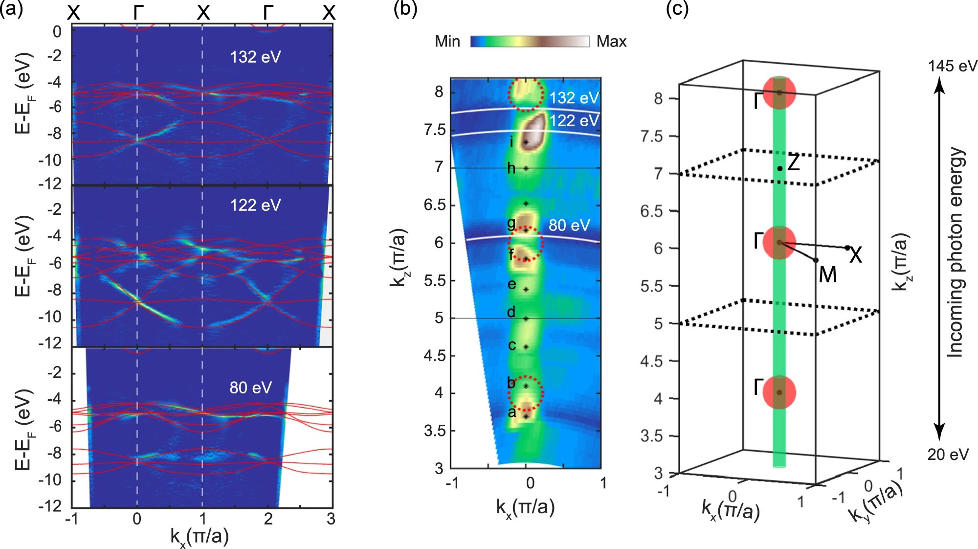

. The measured band structure is overlaid with the LQSGW band structure calculated for bulk BaSnO<sub>3</sub>. The measured and calculated bands show good agreement, with a clear dispersion along <i>k</i><sub><i>z</i></sub>. <b>b</b> Intensity map at the Fermi energy in the plane perpendicular to the sample surface (<i>k</i><sub><i>x</i></sub>–<i>k</i><sub><i>z</i></sub>), measured with incoming photon energies ranging from 20 to 145 eV. No clear periodicity is evident along <i>k</i><sub><i>z</i></sub>. The black squares indicate the Brillouin zone boundaries as inferred by the periodicity of the valence bands shown in panel (<b>a</b>), using the LQSGW calculations as a reference. The red circumferences mark the expected bulk Fermi surface centered at the Γ points (<b>c</b>) Sketch illustrating the difference between the measured and calculated Fermi surfaces. The calculated 3D sphere-like Fermi surface with Fermi momentum <i>k</i><sub><i>F</i></sub> based on the nominal doping of the film is shown in red, while the measured 2D cylinder-like Fermi surface with <i>k</i><sub><i>F</i></sub> based on the measurements results is shown in green. ARPES intensity follows the attached color scale bar. Credit: <i>Communications Physics</i> (2022). DOI: 10.1038/s42005-022-01091-y")
Novel materials could revolutionize computer technology. Research conducted by scientists at the Paul Scherrer Institute PSI using the Swiss Light Source SLS has reached an important milestone along this path.
Microchips are made from silicon and work on the physical principle of a semiconductor. Nothing has changed here since the first transistor was invented in 1947 in the Bell Labs in America. Ever since, researchers have repeatedly foretold the end of the silicon era—but have always been wrong.
Silicon technology is very much alive, and continues to develop at a rapid pace. The IT giant IBM has just announced the first microprocessor whose transistor structures only measure two nanometers, equivalent to 20 adjacent atoms. So what’s next? Even tinier structures? Presumably so—for this decade, at least.
At the same time, new ideas are taking shape in research laboratories regarding a revolutionary technology that could turn everything we think we know about microelectronics on its head. One of the shining lights in this research field is provided by Milan Radovic’s team. Milan Radovic works at the Paul Scherrer Institute and his team just published an article in the journal Communications Physics presenting sensational findings from cutting-edge research into transparent oxides (TOs) that could open up huge prospects for this novel technology.
Innovative microchips
Radovic and his co-authors Muntaser Naamneh and Eduardo Guedes, together with the Bharat Jalan research group from the University of Minnesota do not work with silicon, but with transition metal oxides (TMOs). These exhibit exotic properties and multifunctional phenomena such as high-temperature superconductivity, colossal magnetoresistance, metal-insulator transition and much more besides. What may initially sound bewildering to a lay person promises enormous advances for the chip technology of the future.
In their latest publication, the researchers focus on barium tin oxide (BaSnO3), a material that combines optical transparency with high electrical conductivity.
Scientists have been trying for some time to elicit semiconductor-like properties from transition metals as well as special transparent oxides such as BaSnO3 and strontium stannate (SrSnO3). Compared with silicon, they offer ground-breaking advantages for optoelectronic elements: these transparent, conductive perovskite oxides, would make it possible to create switching elements with directly linked electrical and optical properties. It may then be conceivable to produce transistors that can be switched with light.
Knowledge of interfaces is critical
All microchips are made from a combination of different substances. To understand their function, it is important to know what happens in the thin adjacent layers, or interfaces, between these materials, because the physical properties of many materials are completely different on the surface compared with their interior.
“Exotic phases” can occur at the interfaces of materials—a discovery made by three British physicists who were awarded the Nobel Prize in 2016. The article just published describes significant advances in the understanding of the surface-state electronic properties of BaSnO3.
The researchers used angle-resolved photoemission spectroscopy at the beamline of the Swiss Light Source SLS to “discover the two-dimensional electronic state of BaSnO3 , which opens up new prospects for this class of materials,” says Eduardo Guedes.
Now the researchers want to find out which other materials exhibit similar properties and could be potential candidates for the optical microchips of the future.
But silicon is far from being an outdated technology, Milan Radovic says. It is in fact highly developed and efficient. “However, technology based on transition metal oxides is much more powerful and versatile—its time will come.”
Muntaser Naamneh et al, Low-dimensional electronic state at the surface of a transparent conductive oxide, Communications Physics (2022). DOI: 10.1038/s42005-022-01091-y
Citation:
New materials for the computer of the future (2022, December 8)
retrieved 8 December 2022
from https://techxplore.com/news/2022-12-materials-future.html
This document is subject to copyright. Apart from any fair dealing for the purpose of private study or research, no
part may be reproduced without the written permission. The content is provided for information purposes only.
For all the latest Technology News Click Here
For the latest news and updates, follow us on Google News.