Novel memory technology based on compound semiconductors

A pioneering type of patented computer memory known as ULTRARAM has been demonstrated on silicon wafers in what is a major step towards its large-scale manufacture.
ULTRARAM is a novel type of memory with extraordinary properties. It combines the non-volatility of a data storage memory, like flash, with the speed, energy-efficiency and endurance of a working memory, like DRAM. To do this it utilizes the unique properties of compound semiconductors, commonly used in photonic devices such as LEDS, laser diodes and infrared detectors, but not in digital electronics, which is the preserve of silicon.
Initially patented in the US, further patents on the technology are currently being progressed in key technology markets around the world.
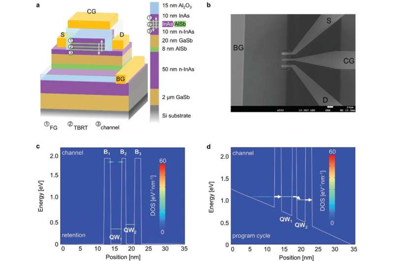
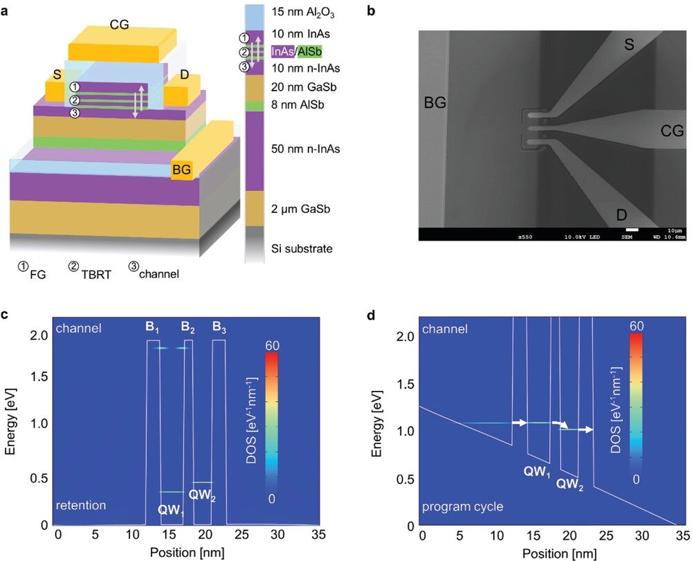
Now, in a collaboration between the Physics and Engineering Departments at Lancaster University and the Department of Physics at Warwick, ULTRARAM has been implemented on silicon wafers for the very first time.
Professor Manus Hayne of the Department of Physics at Lancaster, who leads the work said, “ULTRARAM on silicon is a huge advance for our research, overcoming very significant materials challenges of large crystalline lattice mismatch, the change from elemental to compound semiconductor and differences in thermal contraction.”
Digital electronics, which is the core of all gadgetry from smart watches and smart phones through to personal computers and datacentres, uses processor and memory chips made from the semiconductor element silicon.
Due to the maturity of the silicon chip-making industry and the multi-billion dollar cost of building chip factories, implementation of any digital electronic technology on silicon wafers is essential for its commercialisation.
Remarkably, the ULTRARAM on silicon devices actually outperform previous incarnations of the technology on GaAs compound semiconductor wafers, demonstrating (extrapolated) data storage times of at least 1000 years, fast switching speed (for device size) and program-erase cycling endurance of at least 10 million, which is one hundred to one thousand times better than flash.
The research is reported in the journal Advanced Electronic Materials.
First steps towards revolutionary ULTRARAM memory chips
Peter D. Hodgson et al, ULTRARAM: A Low‐Energy, High‐Endurance, Compound‐Semiconductor Memory on Silicon, Advanced Electronic Materials (2022). DOI: 10.1002/aelm.202101103
Citation:
Novel memory technology based on compound semiconductors (2022, January 7)
retrieved 7 January 2022
from https://techxplore.com/news/2022-01-memory-technology-based-compound-semiconductors.html
This document is subject to copyright. Apart from any fair dealing for the purpose of private study or research, no
part may be reproduced without the written permission. The content is provided for information purposes only.
For all the latest Technology News Click Here
For the latest news and updates, follow us on Google News.

