Radiofrequency transistors based on high-purity carbon nanotube arrays

Most next generation wireless communication technologies require integrated radiofrequency devices that can operate at frequencies greater than 90 GHz. Two of the semiconductors most widely used to fabricate radiofrequency devices are silicon complementary metal-oxide-semiconductor (CMOS) field-effect transistors (FETs) and transistors based on III-V compound semiconductors, particularly GaAs.
Both these semiconductor RF technologies, however, are unable to simultaneously achieve high operating frequencies and be easy to integrate within wireless communication technologies. A promising candidate for the development of high-speed FETs (up to terahertz frequencies) are semiconducting single-wall carbon nanotubes (CNTs), due to their favorable electronic and physical properties. Remarkably, the material requirements of CNTs for the fabrication of RF analog and digital devices are almost the same.
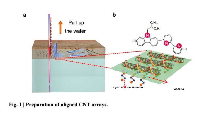
Researchers at Peking University in China have recently fabricated new RF transistors based on aligned CNT arrays. These transistors, presented in a paper published in Nature Electronics, were created using two distinct methods, a double-dispersion sorting and a binary liquid interface aligning process.
“CNT FETs could achieve better performance for SoC applications than silicon and III-V compound semiconductors-based technologies,” Lianmao Peng, one of the researchers who carried out the study, told TechXplore. “However, both the speed and gain of CNT FETs still lag behind theoretical predictions.”
The speed of CNT-based FETs has so far been limited and unsatisfactory, primarily due to a lack of well-aligned semiconducting CNT arrays with a suitable density, high uniformity, high semiconducting purity and high carrier mobility. To overcome these challenges and develop highly performing CNT RF devices, the researchers decided to adapt the structure of the CNT materials.
To fabricate their RF transistors, Peng and his colleagues mainly used two processes known as electron beam lithography (EBL) and atomic layer deposition (ALD). They then completed the preparation of each of the functional layers in the devices using other nano-fabrication equipment, via what is known as a top-down lift-off process.
“We obtained CNT arrays for radiofrequency application through a double-dispersion and binary liquid interface-confined self-assembly (BLIS) procedure and realized the fabrication of highly performing radiofrequency devices and amplifiers based on CNT arrays,” Peng said. “As for our primary objectives, we wished to explore the potential of upper-limit frequency, the power gain and linearity performance potential of CNT array-based transistors and amplifiers under the experimental conditions.”
The nanotube arrays developed by Peng and his colleagues have a density of approximately 120 nanotubes per micrometer, exhibiting a carrier mobility of 1,580 cm2V-1s-1 and a saturation velocity of up to 3.0×107 cm s-1. Using these nanotube arrays, the researchers fabricated FETs that achieved a high d.c. performance when operating at millimeter-wave and terahertz frequencies.

“We hope that the speed, amplification and linearity potential of the CNT RF devices can be truly demonstrated in experiments,” Peng said.
Notably, the CNT-based RF transistors developed by this team of researchers fall into the category of metal-oxide-semiconductor (MOS) field-effect transistors (FETs). In other words, the mechanism underpinning their operation resembles the one enabling the operation of MOSFETs.
“The RF transistor is a three-terminal device, consisting of a gate node, source node and drain node,” Peng said. “The gate node controls the conductivity channel between source and drain node.”
To enable the amplification of radiofrequency signals, the transistors created by the researchers rely on the transconductance amplification of the FET device. Moreover, their speed of operation depends on the transportation speed of carriers in the device channel.
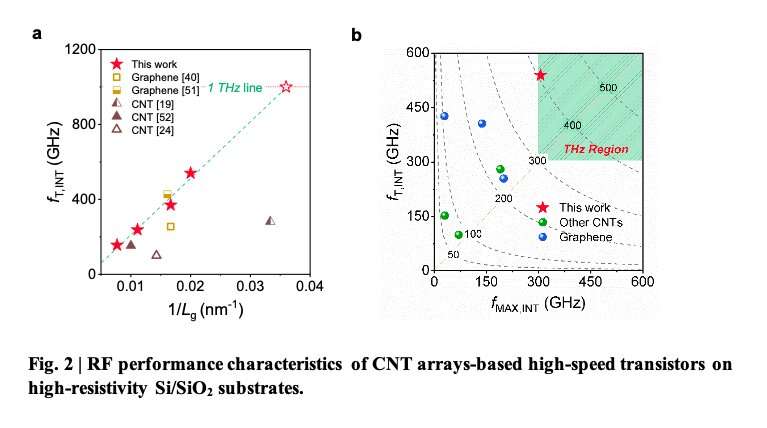
“The main advantages of our transistors can be summarized as three main points,” Peng said. “Firstly, our devices based on high-density semiconducting CNT arrays show the strong on-state driving capability, leading to large transconductance and large current, which brings the strong RF signal amplification capability. Secondly, our CNT arrays exhibit high carrier saturation speed and high mobility, corresponding to the high current gain cut-off frequency (fT) and power gain cut-off frequency (fMAX).”
In initial evaluations, the CNT arrays created by Peng and his colleagues were found to be of excellent quality and exhibited a high inherent linearity performance. Remarkably, the researchers were the first to push the intrinsic frequency performance of CNT-based RF FETs into the terahertz regime.
“While it was long predicted theoretically that CNT FETs have THz potential, our results are the closest experiment demonstration of this,” Peng said. “Also, CNT arrays-based FETs devices exhibit higher cut-off frequencies than silicon-based devices under the similar gate length and same de-embedding conditions.”
The findings gathered by this team of researchers demonstrate that the RF speed of CNT-based devices can reach desirable levels outlined by theoretical predictions. In the future, Peng and his colleagues would like to improve the performance of CNT-based RF transistors even more, by optimizing their composition and structure further.
“We also plan to realize practical CNT-based amplifiers operating at the terahertz regime,” Peng said. “By integrating them with high-performance digital CNT-based CMOS ICs, we look forward to applying CNT arrays-based high-speed electronics to SoC applications operating in millimeter wave and even THz frequencies.”
Researchers create a hybrid technology that combines III-V tunnel FETs and MOSFETs
Radiofrequency transistors based on aligned carbon nanotube arrays. Nature Electronics(2021). DOI: 10.1038/s41928-021-00594-w
© 2021 Science X Network
Citation:
Radiofrequency transistors based on high-purity carbon nanotube arrays (2021, July 9)
retrieved 9 July 2021
from https://techxplore.com/news/2021-07-radiofrequency-transistors-based-high-purity-carbon.html
This document is subject to copyright. Apart from any fair dealing for the purpose of private study or research, no
part may be reproduced without the written permission. The content is provided for information purposes only.
For all the latest Technology News Click Here
For the latest news and updates, follow us on Google News.

