Wafer-scale transistor arrays created using slot-die printing

Engineers have been trying to devise increasingly efficient and low-cost methods to fabricate electronic components and devices on a large-scale. Recently, some studies explored the possibilities of creating electronics using solution processing techniques, which involve the deposition of materials with electrical properties from a solution onto a surface.
Researchers at Yonsei University and Sungkyunkwan University in South Korea recently fabricated wafer-scale transistor arrays based on the inorganic compound molybdenum-disulfide using a solution processing method. Their paper, published in Nature Electronics, could contribute to enabling the large-scale and low-cost fabrication of next-generation electronics.
“We have been working on solution-processed 2D nanomaterials for scalable electronic applications for years, yet satisfying both electronic performance and scalability based on solution-based approaches has been very challenging until now,” Joonhoon Kang and Jeong Ho Cho, co-authors of the paper, told Tech Xplore.
“Our previous work, published last year in Advanced Materials, focused on demonstrating wafer-scale electronics based on various solution-processed 2D materials. Building on this study, the primary goal of our new work was to maximize electronic properties without compromising scalability.”
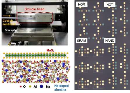
To fabricate their wafer-scale transistors, Kang, Cho and their colleagues used a commercial slot-die printing process. This is a technique for depositing liquid materials onto different substrates, such as glass, metals or polymers.
The researchers created inks containing nanosheets of molybdenum disulfide and sodium-embedded alumina. They then used slot-die printing to deposit these inks on a substrate, creating semiconducting and gate dielectric layers.
“For large scalability, we firstly utilized a slot-die coater, which is an industrial-level coating method, to cover solution-processed dielectric and semiconducting channel layers over 5-inch wafer with high uniformity,” Cho and Kang explained. “In addition, to demonstrate high-performance electronics, we utilized a unique dielectric layer, sodium-doped alumina, which enables highest field-effect mobility (>100 cm2/Vs) based on solution-processed MoS2 thin-films.”
In initial evaluations, the transistors created by the researchers performed remarkably well, exhibiting average charge carrier mobilities of 80.0 cm2 V−1 s−1 in field-effect transistor measurements and 132.9 cm2 V−1 s−1 in Hall measurements at room temperature. To demonstrate their transistors’ potential further, Cho, Kang and their colleagues used them to create various different devices, including NOT, NOR, NAND and static random-access memory.
In the future, their work could inspire other research teams worldwide to explore the potential of solution processing techniques for the fabrication of electronics. These efforts could collectively help to identify new processes for fabricating electronics on a large-scale.
“The most important contribution of this work is that it provides a novel route for high-performance 2D material-based electronics in large-scale using an industrial-level coating technique,” Cho and Kang added. “In our next studies, we plan to expand solution-processed material candidates with different electronic properties such as electronic type, bandgap, etc., which could be utilized for various electronic applications.”
More information:
Yonghyun Albert Kwon et al, Wafer-scale transistor arrays fabricated using slot-die printing of molybdenum disulfide and sodium-embedded alumina, Nature Electronics (2023). DOI: 10.1038/s41928-023-00971-7
© 2023 Science X Network
Citation:
Wafer-scale transistor arrays created using slot-die printing (2023, June 27)
retrieved 27 June 2023
from https://techxplore.com/news/2023-06-wafer-scale-transistor-arrays-slot-die.html
This document is subject to copyright. Apart from any fair dealing for the purpose of private study or research, no
part may be reproduced without the written permission. The content is provided for information purposes only.
For all the latest Technology News Click Here
For the latest news and updates, follow us on Google News.
