Perovskite light-emitting diodes toward commercial full-color displays: Progress and key technical obstacles
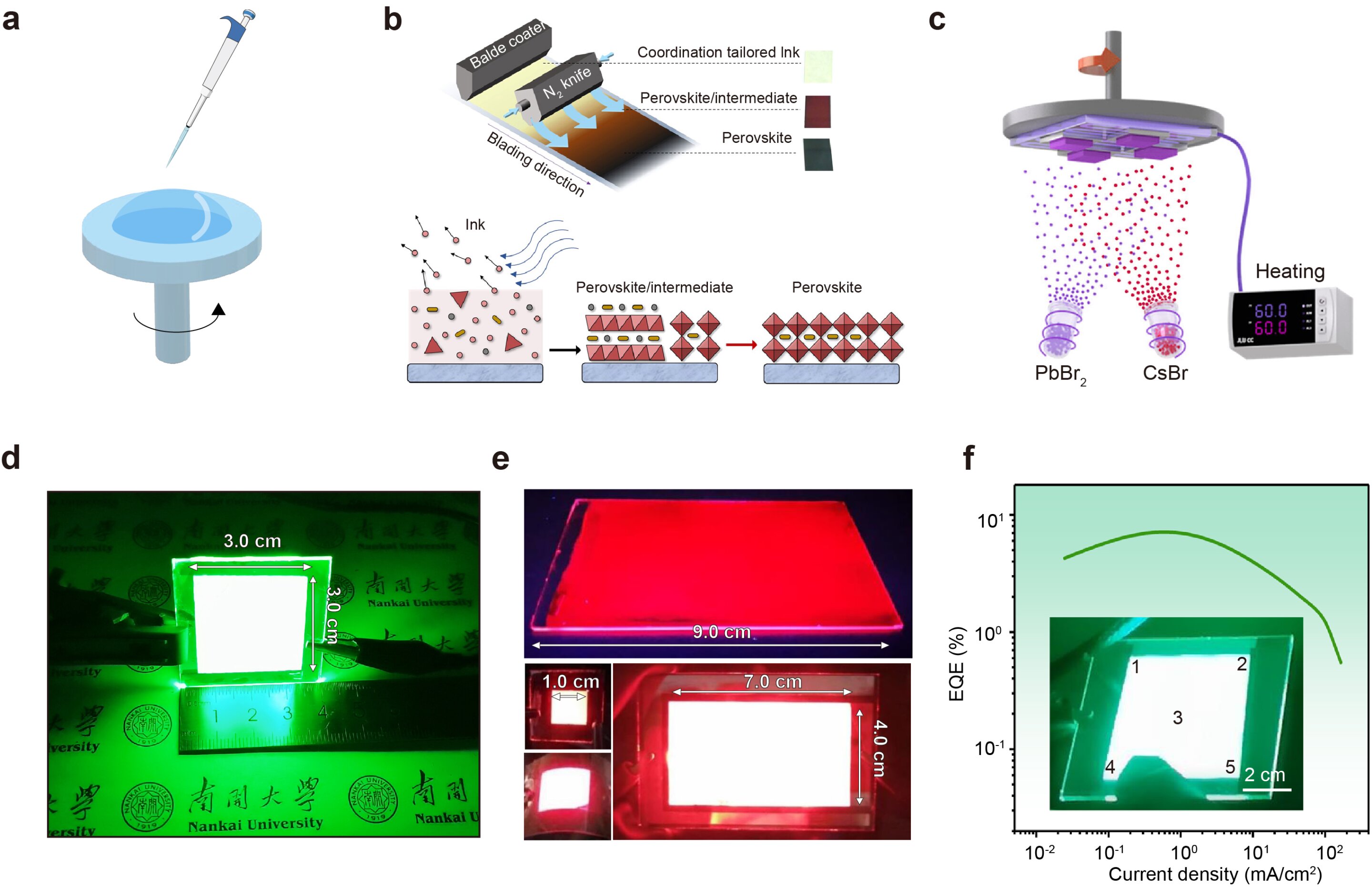
, blade-coating (b), and vapor deposition (c); Large-area PeLED devices based on spin-coating (d), blade-coating (e), and vapor deposition (f). Credit: Changjiu Sun, Yuanzhi Jiang, Keyu Wei, Mingjian Yuan")
Perovskite light-emitting diodes (PeLEDs) have been considered the most potential application technologies for the next-generation display and lighting field. Since the first room temperature-emission PeLED was demonstrated in 2014, the performances of PeLEDs have improved rapidly within a few years. The external quantum efficiencies (EQEs) of green, red, and near-infrared emission devices have exceeded 20%.
Recently, the EQEs of blue PeLEDs have also exceeded 17%. PeLEDs have shown performance indicators constantly approaching the state-of-the-art organic and quantum dot LEDs, and exhibited unique advantages in terms of color purity, material cost, and preparation process.
Despite the fantastic progress, several challenges exist for PeLEDs to achieve commercial display applications.
On the one hand, the high-performance PeLEDs only worked in small active areas. When the active area expands, high nonuniformity of large-area active layers is the major obstacle. On the other hand, most researches on PeLEDs concentrate on prototype devices with a single emission pixel.
However, lagging in the technology of high-resolution, full-color perovskite array patterning strategies and device integration technologies, the step of PeLED displaying commercialization is strongly impeded. In addition, high-performance PeLEDs are mainly prepared based on rigid substrates, thus limiting their potential application scenarios. Perovskite materials have solution-processable properties and intrinsic mechanical flexibility, which provides the prospects for preparing perovskite-based flexible optoelectronic devices.
In a new paper published in Light: Advanced Manufacturing, a team of scientists, led by Professor Mingjian Yuan from Key Laboratory of Advanced Energy Materials Chemistry (Ministry of Education), Renewable Energy Conversion and Storage Center (RECAST), College of Chemistry, Nankai University, China, and co-workers summarizes the representative attempts for PeLEDs in commercial display applications, and discusses the key challenges as well as development prospects in this field.
They outline three significant technical obstacles toward the needs of the consumer electronics market and the level of industrial production requirements. This review includes large-area PeLEDs preparation, PeLEDs’ patterning strategies, and flexible PeLED devices.
 and down-top (b) lithography steps for patterned perovskite arrays; nanoimprinting (c) and imprinting-transfer printing (d) steps for patterned perovskite arrays. Credit: Changjiu Sun, Yuanzhi Jiang, Keyu Wei, Mingjian Yuan")
The large-scale fabrication of PeLEDs is of significant importance towards display panels. High-performance PeLED devices demonstrated in lab-scale production usually have only a few square millimeters of emission area. When enlarging the emission region, the perovskite film shows decreased crystallinity and uniformity, resulting in low device performance.
These drawbacks make PeLEDs challenging to transfer their excellent electroluminescence (EL) features into scalable manufacturing lines. To achieve large-area and high-throughput production of the devices, developing feasible large-area perovskite film depositing technology is of necessity. It includes improving the existing spin-coating method and using large-scale compatible depositing technologies such as new-type blade-coating or vapor deposition methods.
Micro- or nano arrays and their fabrication methods are essential for developing advanced integrated optoelectronic platforms. Precise and highly integrated pixels are prerequisites for incorporating these emerging perovskite materials into full-color high-resolution displays. Tremendous efforts have been devoted to developing structured perovskite films, and demonstrating these obtained optical films in laser, super-surface, and nonlinear optic devices. However, integrating the patterned perovskite films into full-color, high-resolution electroluminescent devices remains challenging.
Delivering high-performance patterned PeLEDs requires pattern strategies compatible with the existing workflows in LED device building, and achieves the unification of high optical performance and low electrical loss. In this section, the authors focus on the attempts to apply patterned perovskite arrays on LED devices. They introduce the pattern strategies of the high-resolution perovskite active layer. These include mask-assisted photolithography technologies, mask-free jet printing methods, nanoimprinting, and transfer printing strategies.
; Young's modulus of perovskite materials along different crystal planes (b); several typical flexible electrodes. Credit: Changjiu Sun, Yuanzhi Jiang, Keyu Wei, Mingjian Yuan")
Flexible LEDs have become revolutionary devices for their various potential applications, such as portable wearable displays and biomedical imaging. In this section, the authors briefly introduce the progress of Flexible PeLEDs. They describe mechanical property regulation strategies for perovskite emitting layers in flexible and stretchable devices. The relationship between structural optimization and material optoelectronic properties is also explained. They review electrode materials compatible with FPeLEDs, such as structured metals, conductive polymers, low-dimensional carbon materials and their composites.
Comprehensive improvement strategies for these candidate materials’ parameters, such as flexibility, conductivity, and transmittance, are also proposed. They also discuss the interfacial and energy level engineering toward improving these electrodes’ compatibility with the perovskite active layer.
More information:
Changjiu Sun et al, Perovskite light-emitting diodes toward commercial full-colour displays: progress and key technical obstacles, Light: Advanced Manufacturing (2023). DOI: 10.37188/lam.2023.015
Citation:
Perovskite light-emitting diodes toward commercial full-color displays: Progress and key technical obstacles (2023, July 19)
retrieved 19 July 2023
from https://techxplore.com/news/2023-07-perovskite-light-emitting-diodes-commercial-full-color.html
This document is subject to copyright. Apart from any fair dealing for the purpose of private study or research, no
part may be reproduced without the written permission. The content is provided for information purposes only.
For all the latest Technology News Click Here
For the latest news and updates, follow us on Google News.